
Conductive Silicone Keypads Manufacturer
Custom conductive silicone keypads for electronic interfaces that require tactile input and electrical switching. SKF develops the keypad structure, conductive contacts, PCB interface, graphics and mounting features around your product requirements. Our engineers consider conductive contact alignment, actuation force, key travel, web geometry and housing integration together to support consistent keypad operation from prototype development through mass production. OEM and ODM projects can be developed from customer drawings, PCB or FPC layouts, existing samples or defined technical requirements.
What Are Conductive Silicone Keypads?
Conductive silicone keypads are molded silicone interfaces that combine tactile key structures with conductive contacts for electrical switching. When a key is pressed, the conductive contact moves into the PCB contact area and closes the circuit.
Unlike individual conductive silicone buttons, a conductive keypad normally contains multiple keys in one molded structure. The key layout, web structure, conductive contact positions and mounting geometry are developed together with the electronic interface.
SKF reviews the keypad together with the PCB or FPC, housing and user interface. This helps address mechanical and electrical requirements before tooling rather than treating the conductive contact as an isolated component.
Conductive Silicone Keypad Manufacturing at a Glance
Electrical Interface
Conductive contact size, resistance and position are selected according to the PCB contact layout and switching requirements. Carbon pills are commonly used, while other contact structures can be considered when the project requires them.
Tactile Response
Actuation force, key travel, snap ratio and return behavior are affected by the silicone hardness and web geometry. SKF reviews these factors together because changing one part of the structure can affect both the pressing feel and contact timing.
Keypad Structure
Key height, key pitch, web thickness, diaphragm geometry and perimeter features are developed around the available housing space and assembly method.
Production
Projects can move from drawing review and DFM evaluation through tooling, samples, molding, conductive contact processing, graphic finishing and final inspection. Production requirements are confirmed from the approved design and sample.
Who Uses Conductive Silicone Keypads?
Conductive silicone keypads are used where several tactile controls need to operate through a shared silicone interface. The engineering priorities vary with the equipment and the way the keypad connects to the electronics.

Industrial Control Equipment
Industrial control panels may contain numeric, navigation and function keys in a compact interface. The keypad needs to fit the enclosure while providing clear tactile response and accurate contact with the PCB. SKF can review key spacing, web geometry, conductive pill position and mounting features around the control panel structure. Environmental requirements such as dust, cleaning agents or temperature exposure should be defined according to the actual equipment.

POS, Payment and Access Equipment
Payment terminals, PIN pads, access systems and similar equipment often require compact key layouts with clear tactile feedback and consistent electrical switching. Conductive contacts can be positioned around the PCB layout, while legends, surface finishes and backlighting features can be developed around the user interface.
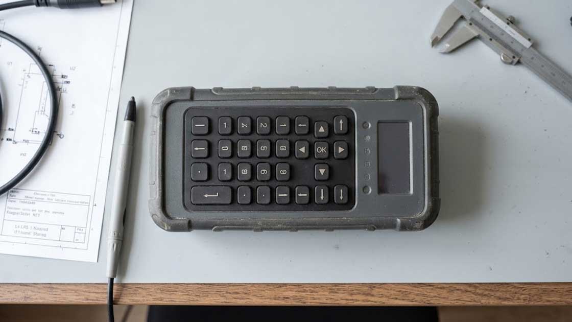
Handheld and Electronic Devices
Handheld controllers, instruments and electronic devices often have limited space for the keypad and PCB. Key pitch, key height and web geometry therefore need to be considered together. A molded conductive keypad can combine numeric, navigation and function keys while keeping the conductive contacts aligned with the underlying circuit.

Automotive and Transportation Controls
Automotive and transportation interfaces can place tighter requirements on available space, tactile response and environmental exposure. SKF can develop compact key layouts with conductive contacts positioned to match the vehicle electronics. The final material and structural requirements depend on the installation location, temperature range, vibration conditions and other customer specifications.

Medical and Laboratory Equipment
Medical and laboratory interfaces may require clear key identification, controlled actuation force and surfaces that can be cleaned according to the equipment procedure. The keypad design can combine conductive contacts with printed or laser-etched legends. Silicone compound, surface treatment and graphic methods should be selected according to the required cleaning conditions and applicable material requirements.
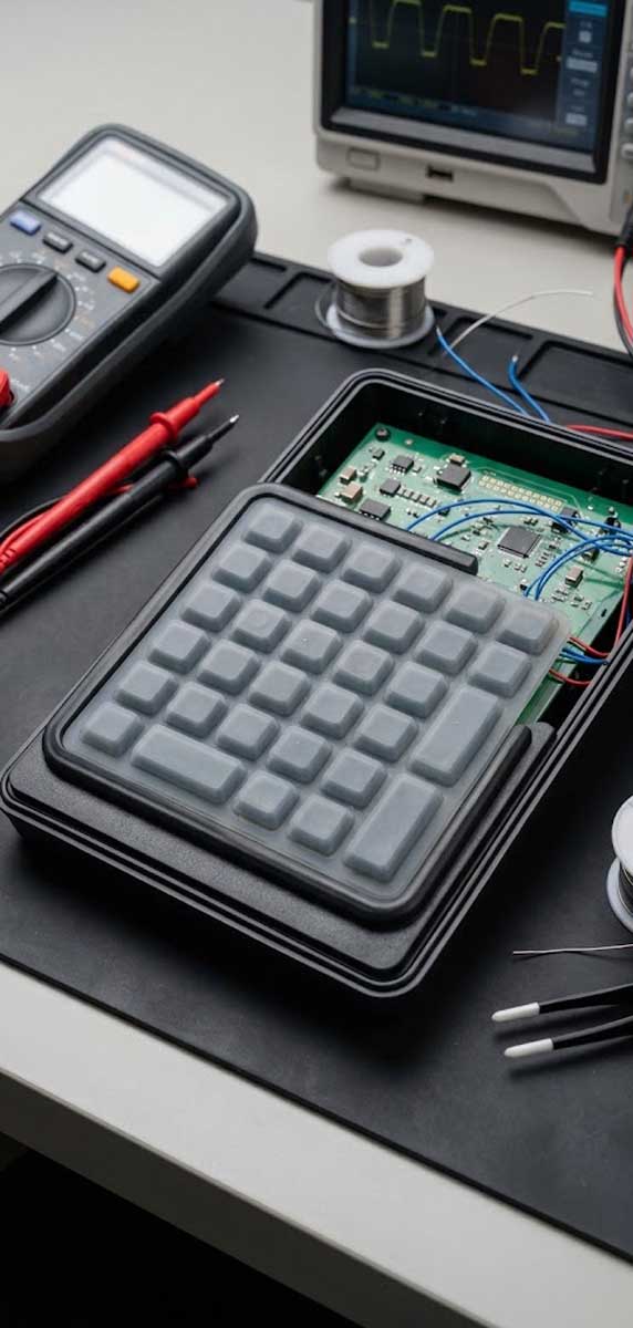
Conductive Silicone Keypad Types We Can Develop
Multi-Function Conductive Silicone Keypad
Directional Navigation Conductive Silicone Keypad
Compact Dual-Color Conductive Silicone Keypad
Function Row Conductive Silicone Keypad
Full Numeric & Function Conductive Silicone Keypad
Standard Numeric Conductive Silicone Keypad
Conductive Silicone Keypad Customization
Conductive keypad customization starts with the electrical interface and mechanical envelope. The conductive contacts cannot be specified separately from the keypad structure because their position and movement are affected by the key geometry.
The overall keypad dimensions, key count, key pitch and key height are developed around the equipment housing and PCB. Mounting holes, locating features and perimeter geometry can also be incorporated when required by the assembly.
Carbon pills are commonly used for silicone keypad switching. Their diameter, thickness, resistance and position need to match the PCB contact design.
The contact should provide enough alignment margin for the intended key movement. The actual resistance requirement should be confirmed from the customer’s circuit and test method rather than assumed from a general product range.
SKF adjusts the silicone web structure to achieve the required actuation force, travel and snap response.
A change in web thickness or geometry can affect the force curve and the point at which the conductive contact reaches the PCB. For this reason, tactile requirements and electrical switching requirements are reviewed together.
Screen printing, pad printing and laser etching can be used for legends and symbols when suitable for the product design. Surface coatings or other finishing methods can also be considered according to the required appearance and use conditions.
For backlit designs, translucent silicone and controlled graphic areas can be incorporated around the lighting system.
Silicone hardness and compound selection affect the keypad structure and tactile response. The appropriate material depends on the operating environment, required force, surface requirements and other project conditions.
Material documentation and compliance requirements should be confirmed for the target market and final keypad configuration.
Start Your Conductive Silicone Keypad Project
Conductive silicone keypads need the electrical contact, tactile structure and mechanical interface to work together. SKF reviews these elements during development so the keypad can be evaluated against the actual product requirements before tooling.
Send your drawing, PCB/FPC layout, sample or available specifications to SKF. Our engineers can review the conductive contact, keypad structure and manufacturing requirements for your OEM or ODM project.
How Should Conductive Silicone Keypads Be Specified?
A conductive keypad should be specified as a complete interface rather than by contact resistance alone.
Actuation Force and Key Travel
Actuation force determines how much pressure the user applies before the key activates. Key travel affects the movement available before and after electrical contact.
The target should reflect the user group, pressing frequency, key size and available mechanical space. SKF can review the force and travel requirements together with the web structure.
Snap Ratio and Return Behavior
Snap ratio describes the relationship between the initial peak force and the lower force after the web collapses. It influences how clearly the user feels the transition during a key press.
Return behavior also affects repeated operation because the key needs to return sufficiently before the next activation. The appropriate values depend on the key geometry and application.
Conductive Contact Position
The conductive contact must align with the PCB contact area during the actual key movement, not only in the static CAD position.
Web geometry, key deformation, molding tolerances and assembly position can all influence this relationship. SKF reviews these elements together during design evaluation.
PCB Contact Pattern
The PCB contact area determines the required contact size and position. A contact that is too small can reduce the available alignment margin, while an unnecessarily large contact may create clearance problems with nearby circuits.
For this reason, the PCB drawing or contact layout is important when developing a custom conductive keypad.
Housing and Mounting Interface
The keypad must fit the enclosure without unwanted interference. Key height, overall thickness, locating features and perimeter geometry should be checked against the housing and PCB assembly.
Conductive Contact and Material Options
Carbon pills are a common conductive structure for silicone keypads. The required resistance, contact size, thickness and position depend on the PCB design and electrical requirements.
SKF can review the carbon pill geometry together with the key structure to help maintain the intended contact area throughout the key stroke.
Other conductive contact structures may be considered when a project has specific electrical requirements. The selection depends on the circuit, contact geometry, available space, manufacturing process and target performance.
The final contact specification should be confirmed against the customer’s electrical requirements and validation method.
Silicone provides the elastic structure that controls key movement and return. Hardness alone does not determine the final tactile response. Web geometry, key dimensions, diaphragm structure and other design factors also affect the force curve.
The compound should therefore be selected together with the mechanical design rather than treated as an independent specification.
Conductive functionality does not prevent the keypad from using different surface treatments. Screen printing, pad printing, laser etching, coatings and molded graphics can be considered according to the application.
The selected process should account for key geometry, required graphic contrast, cleaning conditions and expected contact with the user’s fingers.
How SKF Develops Conductive Silicone Keypads

Requirement Review
SKF starts with the information that defines the complete interface. This can include the keypad drawing, 3D model, PCB or FPC layout, key functions, electrical requirements, tactile targets, housing information, operating environment and expected quantity. If an existing keypad or sample is available, it can also be reviewed as a reference.
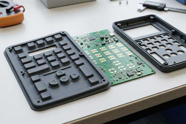
Keypad and DFM Evaluation
The engineering review covers key spacing, web geometry, diaphragm structure, wall transitions, draft, mounting features and demolding requirements. Conductive contact locations receive additional attention because their position must remain suitable for the PCB interface during actual key operation.
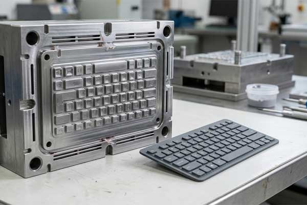
Tooling Development
After the design is confirmed, tooling is developed around the approved keypad geometry and production requirements. Mold details are reviewed for the key structure, web sections, perimeter and other critical features.

Silicone Molding
The approved silicone compound is molded into the keypad structure using the selected production process. Molding conditions and cavity design are controlled according to the product requirements.

Conductive Contact Processing
Conductive contacts are applied or formed according to the approved design. Position, appearance and contact characteristics are checked against the project requirements.

Graphic and Surface Processing
Printing, laser etching, coating or other approved finishing processes are completed after molding as required. Graphic alignment and surface appearance are checked against the approved artwork and sample.
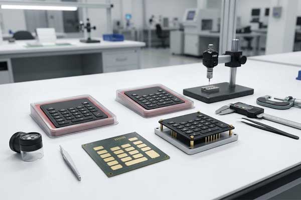
Final Inspection
Finished keypads are checked against the approved specification and sample. Inspection can cover dimensions, appearance, tactile response, conductive contact position, electrical performance, graphics and packaging according to the agreed inspection plan.
Conductive Silicone Keypad Quality Control
Quality control focuses on the parts that affect both mechanical operation and electrical switching.
Dimensional Inspection
Overall dimensions, key height, key pitch, thickness and other critical dimensions are checked against the approved drawing.
Tactile Inspection
Actuation force and travel can be checked using an agreed test method. Different key groups may have different targets when the keypad contains keys with different sizes or functions.
Conductive Contact Inspection
Conductive contact position and appearance are checked against the approved design. Electrical testing can be arranged according to the customer’s contact resistance and switching requirements.
Graphic Inspection
Printed or laser-etched legends are checked for position, size, contrast, completeness and alignment according to the approved sample.
Approved Sample Control
The approved sample provides a production reference for key geometry, color, graphics, tactile response, conductive contact layout, surface finish and other agreed characteristics.
The final inspection standard can follow the customer’s specification or an agreed sampling plan.
Typical Conductive Silicone Keypad Specifications
| Specification | Typical Reference |
|---|---|
| Product | Custom conductive silicone keypad |
| Material | Silicone rubber |
| Silicone hardness | Project-specific, commonly selected within the silicone keypad design range |
| Key layout | Numeric, function, navigation or custom |
| Actuation force | Customer-defined according to key structure |
| Key travel | Customer-defined according to web geometry and PCB interface |
| Snap ratio | Customer-defined according to tactile requirements |
| Conductive contact | Carbon pill or other approved conductive contact |
| Contact resistance | Defined according to the circuit and agreed test method |
| Contact position | Matched to PCB or FPC contact layout |
| Keypad color | Standard or customer-specified |
| Graphics | Screen printing, pad printing, laser etching or molded graphics |
| Surface | Molded texture, matte finish or approved coating |
| Backlighting | Available for suitable translucent designs |
| Mounting | Housing-specific mounting and locating features |
| OEM / ODM | Available |
Final specifications are confirmed from the keypad design, PCB/FPC interface, silicone compound, conductive contact, operating conditions and approved sample.
What Should You Provide for a Conductive Silicone Keypad Quote?
A drawing is the best starting point, especially when the keypad needs to match an existing PCB and housing.
Please provide the available information such as the 2D drawing, 3D CAD file, PCB or FPC contact layout, keypad dimensions, key functions, target actuation force, key travel, conductive contact requirements, operating environment and estimated quantity.
If some specifications are not available, an existing keypad sample or equipment interface can still help SKF evaluate the design. The missing requirements can then be identified during the engineering review.
Frequently Asked Questions
What is the difference between conductive silicone keypads and conductive silicone buttons?
Conductive silicone buttons normally refer to individual conductive button components. Conductive silicone keypads integrate multiple keys, conductive contacts and the supporting silicone structure into one interface. The keypad is therefore developed around the PCB, housing and complete user interface.
Do conductive silicone keypads always use carbon pills?
No. Carbon pills are commonly used, but other conductive contact structures may be considered when the electrical and mechanical requirements call for them. The appropriate option depends on the PCB interface, required resistance, contact geometry and project conditions.
Can SKF match the conductive contacts to our PCB?
Yes. The PCB or FPC contact layout can be reviewed during development. Contact size and position are then considered together with the keypad web structure and key movement.
How is actuation force controlled?
Actuation force is influenced by silicone hardness, web thickness, diaphragm geometry, key dimensions and other structural factors. SKF adjusts the keypad structure according to the customer's target rather than selecting force from the silicone material alone.
Can conductive silicone keypads be backlit?
Suitable designs can use translucent silicone and controlled graphic areas for backlighting. The final result also depends on the LED arrangement, PCB, light guide and internal structure of the equipment.
Can conductive silicone keypads include printed or laser-etched legends?
Yes. Screen printing, pad printing and laser etching can be considered according to the key geometry, graphic requirements and expected use conditions.
What information does SKF need before developing tooling?
The most useful information includes the keypad drawing or 3D model, PCB/FPC contact layout, housing dimensions, key functions, tactile requirements, conductive contact requirements, material requirements and expected quantity.
Can SKF develop a keypad from an existing sample?
An existing keypad can be used as a reference for dimensions, structure, graphics and tactile requirements. The final design still needs to be checked against the current PCB, housing and production requirements.